Hardware details
The design goal was to use as many 'regular TTL parts' as I could. No calculator chips, no microcontrollers. Certainly, this could have easily been built using an Arduino or a RaspberryPi and have even more capabilities, but I wanted more of a challenge.
I decided to use an AMD2901 4-bit processor slice to be similar to the Wang 360's 4-bit BCD processing. My only compromise to modern technology was to use a Teensy 3.2 as the microcode ROM and the MCP23017 parallel I/O port chips. They substituted for 6 1Kx8 EPROMS which would have been a real pain to unplug, erase, program, and replace as I developed the microcode. But, to be clear, the Teensy code just reads in the address from the AMD2910 controller and responds on the I2C port with the contents of that location in microcode ROM.
The block diagram is:

The Teensy responds to requests from the AMD2910 controller with individual microcode words (43-bits wide) sent over the I2C bus to three MCP23017 parallel port expanders.
The microcode words are latched into 74LS374 8-bit latches and distributed to the various chips on the board (more on this later).
In addition to the accumulator and log accumulator in the AMD2901, there is an external 8-digit BCD "Display Register". The contents of this register are held in 74LS175s whose contents are always displayed on the TIL311 display digits. The contents of the display register can be read into the AMD2901 via the 74LS244 tri-state buffers. The TIL311's display digits 0-9 and A-E (not used) and I built external logic so that, if the latch holds binary F, the digit is blanked. This is used for leading zero suppression.
There is one 'state' flip-flop, modeled after the DA flip flop in the Wang 360. The issue is: when a user presses a number key, the required action depends on the state of the display. If this is the first digit of the number being typed, then the display needs to be cleared before showing this new digit. However, if the user is in the middle of entering a number, then the display should not be cleared. If the DA ff is set, it means the display needs to be cleared before the new digit is placed in the display register and the DA ff is then cleared; if the DA ff is cleared, then any typed digits are entered into the display. All mathematical operations set the DA ff when they complete.
There are two 4-bit data buses, one for data to the AMD2901 and one for data from the AMD2901. These are shared by the 74LS175 display register latches, the log ROM, the KB encoder and other misc components as controlled by the "Address or Constant" field ("AorC") of the microword:
The AMD2910 controller responds to several condition codes which are selected using a 74LS151 and can be optionally inverted by microword bits:
The 43-bit microword is assigned as follows:
The log ROM stores 8-digit BCD log values for the log and anti-log calculations.
Because it made it easier for me to think through the algorithms, I converted them all to positive values that I could add or subtract as desired. All are multiplied by 10,000,000 to convert them to 8-digit integers. In the end, I did not need them all - the algorithm is rather economical that way - but I included them early in the design 'just in case'. The ones I used are highlighted - there's a pattern there; for more, see later.
-
Address bits 0-3 select which of the 8 digit values to output
-
Address bits 4-7 select from a list of 8-digit base-10 logarithms:
-
0 = -log(0.9) = 00457575
-
1 = -log(0.99) = 00043648
-
2 = -log(0.999) = 00004345
-
3 = -log(0.9999) = 00000434
-
4 = -log(0.99999) = 00000043
-
5 = -log(0.999999) = 00000004
-
6 = log(1.1) = 00413926
-
7 = log(1.01) = 00043214
-
8 = log(1.001) = 00004341
-
9 = log(1.0001) = 00000434
-
A = log(1.00001) = 00000043
-
B = log(1.000001) = 00000004
-
Schematics are shown below (click on them to see expanded view):
1) The CPU (AM 2901 & AM2910):
This includes the condition code selector and two state flip-flops (one for the display state and one to synchronize the input from the keyboard).

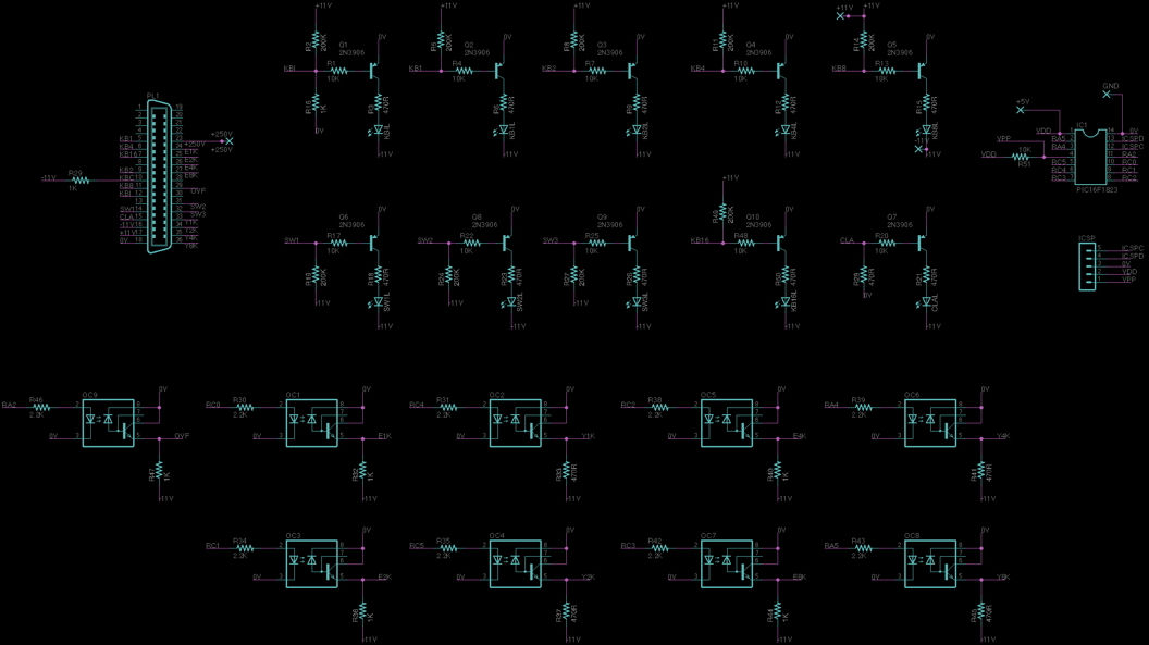
2) The Keyboard Encoder:
The columns are scanned while waiting for a keypress. The encoder ROM's address lines are a combination of the binary column address and the row signals. When a key is pressed, the key's code appears on D0-D3 and a 1 appears on D4 - this then triggers the state machine to change to "have keypress" and set the "Kpress" line until signaled by the CPU that the keypress has been responded to (KB ack).

3) The Teensy, I/O expanders, and pipeline register:

4) The display board decoders, etc:

5) The log ROM:

6) Two sample display digits
