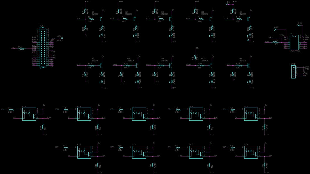
Wang 320 Calculator III - the electronics package
Bringing it back to life 5: Core Driver Voltages
It still wasn't quite working right. The displays showed numbers and there was a response to key presses but not what it was supposed to.
While surfing the web, I found someone selling a #529 board ("Sensing amplifier and G-storage"). This board, among other things, provides regulated voltages for the core driver boards. The core driver voltages are critical for proper core memory function since core memories depend on sending exactly 1/2 the current needed to flip a bit down each of the two wires used to access an individual core (see this site for details). If this "half select current" is too high, some bits will flip when they shouldn't; if it's too low, bits that should flip may not. The e-bay posting said, "Problems with the #529 manifest themselves as random number display, inconsistent keyboard input and display, and inability to perform any calculations." and also mentioned that there is a trimmer potentiometer for adjusting the core drive voltage on the board.
This might be part of the problem. However, it is really not clear what the proper voltages are. At different parts of the schematic, they are listed as "+5.7V and -6V", "+6.2V and -6.2V", and "+6V and -6V". I contacted the seller of the board and some others but received no reply.
So I decided to be empirical: tweak the potentiometer, measure the voltage, and see whether it works or not. First, I noticed that the voltage drops by ~0.45V as the electronics package warms up over about 5-10 minutes. So, I did all the measurements after letting it warm up. Also, the voltages track each other so one potentiometer adjusts both. The results are:
-
-5.95V/? - "Clear display" key doesn't work. Voltage probably too low.
-
-6.2V/+5.6V - seems to work OK
-
-6.4V/+5.8V - also working OK
-
-6.6V/? - no keys work. Voltage too high
So, I set it to -6.17V/+5.6V and it worked as best it could. At this point, I can enter some numbers and some of the function keys work.
Bringing it back to life 6: Some circuit tracing
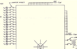
While I was waiting for some parts from Mouser and a circuit board from Seeed studios (fantastic and cheap service, by the way), I decided to get ready for some serious debugging. I removed all the cards and used an ohm-meter to figure out some of the connections. In particular, I wanted to know which keyboard was connected to which keyboard driver board, how the keyboards are selected for attention from the calculator, and which of the core driver boards drove which core lines and where they got their address signals. So I edited the schematics I linked before down to a set of only those boards found in the 320SE and made duplicate pages for each board type that appeared more than once. I then marked up the .pdf with the connections I found. This is posted here.
Bringing it back to life Phase 7: Electronics Package Diagnosis
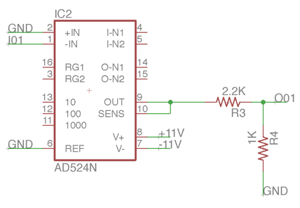
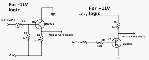
It was clear that I'd need to look at the internal logic signals with the Saleae analyzer. I could have just used the Saleae in analog mode but the resulting files are huge and, in most cases, I only need a binary interpretation. So I need to invert the voltage and reduce it by a factor of 3 and it will be easily readable and interpretable by the Saleae. I had on hand many AD524 Precision Instrumentation Amplifiers. I used them in inverting configuration and hooked their output to a 1/3 voltage divider. Note that I ended up using a +/- 15V supply for the AD524's instead of the labeled +/- 11V supply so that the output voltage wouldn't clip. In the schematic "I01" is an input from the 320 and "O01" is the corresponding output to the logic analyzer. NOTE that you must use the "1.2V logic level" on the Saleae for proper results.
I built a board with 16 of these and a 20-pin header to connect the Saleae LogicPro 16. The input connectors ere tricky. Neither alligator clips nor the clips that came with the Saleae make stable connections to the wiring pins on the 320 Electronics Package. I found that little connector pins Amphenol 66181-1’s (Mouser 571-66181-1) fit really nicely and snugly over the 320's pins and they are easily connected with wire and insulated with heat-shrink tubing. The completed rig looks like this (inputs to the left; output pins on right):

I next needed to look carefully at what was working and what wasn't.
-
What was working:
-
For all 4 keyboards, you could "Clear display" (sets all digits to blanks) and "Clear all" (sets all digits to 0's).
-
so the clearing works and all registers can be set to all 0's or all blanks
-
-
You could enter at least a few numbers on each keyboard
-
so the input routine is at least partly working
-
-
once set, a number was stable
-
since reading core memory is destructive, this meant that (most likely) all the cores could be written to and read from
-
-
entering numbers or hitting other buttons on one keyboard had no effect on the others
-
so there isn't any crosstalk
-
-
can enter and recall short (see later) numbers into the accumulators
-
so those registers are OK
-
-
-
What wasn't working:
-
addition and subtraction were OK for the first few significant digits but not the ones to the right
-
hitting Enter or any of the log-related keys sent it into lala land - the display would keep changing and only a "prime" would get it to stop
-
I started a systematic analysis and saw that there was clearly something wrong with the 6th digit from the left (location 9 in core):
-
You could enter digits up to there but not past there. That is, keying in 1, 2, 3, 4, 5, 6, 7, 8, 9, 0 displayed "+12345xxxxx" ("x" = a blank digit)
-
Addition had strange behavior around digit 6 (underlined below)
-
Clear all => "+.00000 00000"
-
Clear display => "+xxxxx xxxxx"
-
2 => "+2xxxx xxxxx"
-
Left + => "+2.0000 70000" - where'd the 7 come from?
-
Left + => "+4.0001 50000" - 2+2 = 4 but 7+7 isn't 15???
-
Left + => "+8.0004 x0000" ??
-
and so on
-
This was true for all 4 keyboards - which pointed to that particular row or column in the core. But it can't be the cores, since we can store "0", "x", "5", and "7" (at least) in those locations. It can't be the register selection, since all the registers work with this one exception. It can't be the read and write registers and drivers since you can read and write fine to the other locations. This left the particular column in the core that holds this digit - either the driver was bad and/or the wires on the core board were bad. Alternatively, something could be wrong with the counters as they try to write data to this location.
How is the memory organized?
It is 1024 bits, organized as 16x16x4. That is, there are 16 registers, each consisting of 16 4-bit BCD digits. There are 4 separate calculating units, each with 4 registers (Working register, Log register, Right accumulator and Left Accumulator). The physical cores are arranged as 4 16x16 arrays. The 16 columns (X-coordinate) correspond to individual registers; the 16 rows (Y-values) correspond to individual digits within each register. When the calculator selects a particular X-Y pair (digit within a register) all 4 bits are read out in parallel on the 4-bit data bus.
The correspondence between X-Y addresses and actual row-column locations is complicated. This is done to avoid crosstalk between sequentially-accessed core locations. As a result, it took some figuring to get access to signals that gave meaningful X and Y coordinates. In the data that follow, the X and Y coordinates are those used by the internal logic, not the physical X-Y locations in the core. More on that later...
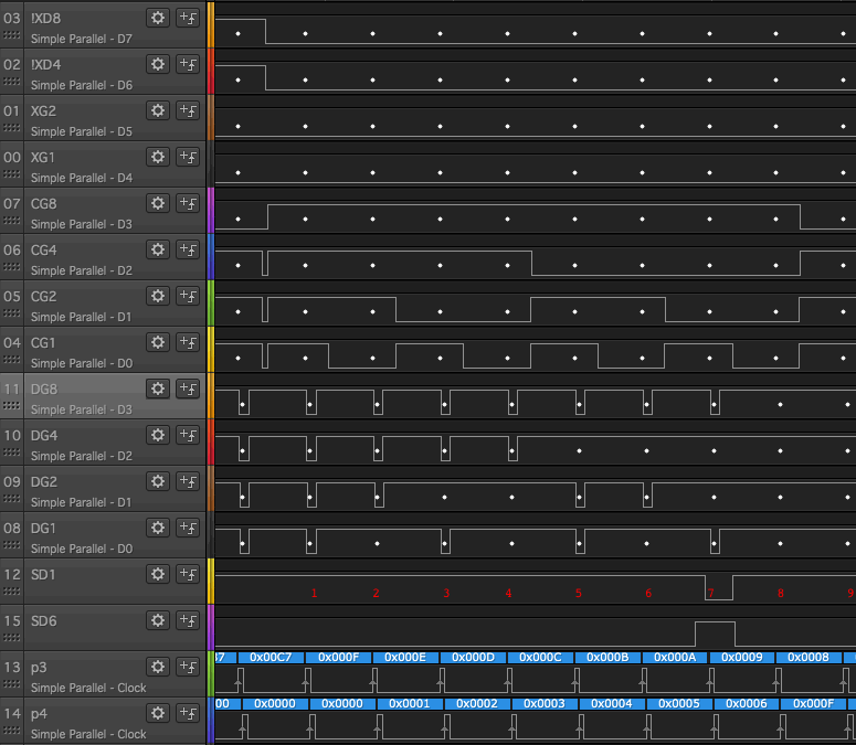
In the image below, the X-coordinates correspond to particular registers. In this case the register selection works like this: !XD8 ("not XD8") and !XD4 are 00 - indicating calculating unit 0; XG1 and XG2 are 00 - indicating the working register (the register that is displayed). The Y-coordinates are determined by the CGx signals - these are the output of the "C-switch" which selects the source of the memory address signals.
The DGx lines are the outputs of the "D-switch" - the data being written to the core. When SD1 is high, the data to be written to the core come from the E-register, which contains the data last read from the core. That is, when SD1 is high, data from the core are read out and written back unchanged to the core. When SD6 is high, data from the 4 least significant bits of the K-register - the data from the keyboard - are written to the core.
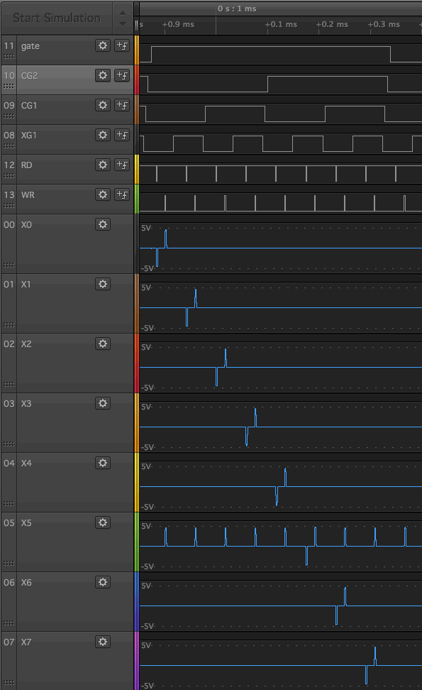
The sequence shown below follows typing "1", "2", "3", "4" and "5" - these were entered successfully. It shows in detail the events following typing "6". The calculator counts down (moving left to right in the digits) through the core starting at location 15 and re-writes the data found there (SD1 high) until it hits the first empty location indicated by a value of 1111 (F). It then writes the keyboard data at that location (SD6 high) and finishes re-writing the remaining digits (SD1 high).
The display should start with "+12345 xxxxx" and end with "+12345 6xxxx".
The numbered events on the right correspond to the red numbers in the figure.
-
Writes a "0" back to location F - the "sign digit" => "+"
-
Writes a "1" back from the core to location E - the most significant digit
-
Writes a "2" back to location D - the second digit
-
Writes a "3" back to location C - the third digit
-
Writes a "4" back to location B - the 4th digit
-
Writes a "5" back to location A - the 5th digit
-
Writes a "6" from the keyboard to location 9
-
Writes an "x" back to location 8 - the next blank digit
-
etc.
The most important part of all that is step 7 where the calculator tries to write "6" to location 9 - it's trying to do the right thing but that "6" is somehow not getting written into the core. So, the problem is not with the counters or switches or logic but with the circuitry that accesses the core.
Bringing it back to life Phase 8: Core driver board repair
The next step was to look at the core driver boards. As I said above, the relationship between address and location is not simple. A Y-coordinate of 9 does not correspond to the 9th row in the core. After tracing the circuit, I found that the 4 CGx lines are inverted before going to the core driver boards as the 4 YDx lines, so an address of 1001 becomes 0110. Then, the bit lines are scrambled to avoid crosstalk (See "Electronic Digital Computers" by Charles VL Smith 1959 for details) like this:
-
The YD8 bit controls the gate line for X-Y driver boards 4 and 5 in the calculator
-
a value of 0 for this bit (!YD8) enables X-Y driver board 5
-
-
The YD4 bit controls the 1's bit on X-Y driver board 5
-
The YD2 bit controls the 4's bit on X-Y driver board 5
-
The YD1 bit controls the 2's bit on X-Y driver board 5
The net result is that a CGx address of 9 (1001) corresponds to address 101 (Y5) on X-Y driver board 5. Phew!
The next logical step was to look at the Y5 driver line from X-Y driver board 5 and see if it was incorrect. I hooked up the Saleae to all 8 of the Y-driver lines from board 5 and saw this:
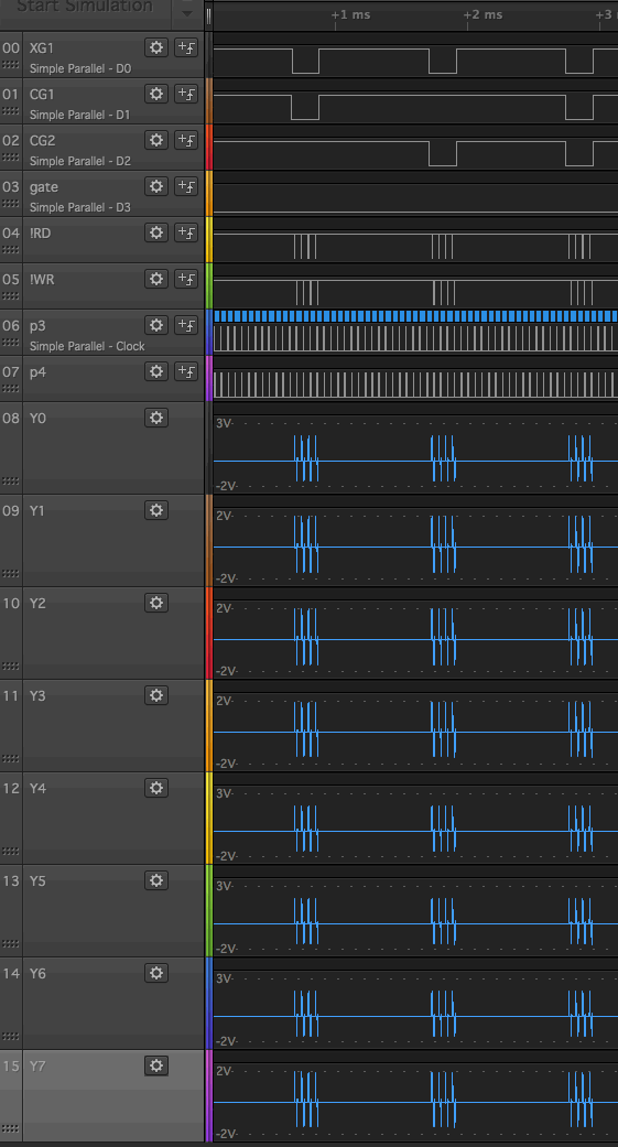
No matter what address (gate, XG1, CG1, and CG2), all 8 Y-driver lines show the same signal!! How is this possible? You can't write to all locations all the time!!
Then I looked at the schematic of the core board...
All the Y-lines are connected together to a single R15 current-limiting resistor. So, while current is flowing through only one Y-line at at time, the voltage from each driver is the same at all Y-lines.
So, it's not possible to see if the drivers are OK with the core driver board in the calculator.
The next step was to build a test-bed for the core driver boards so I can test them outside of the calculator.
This requires several things:
-
Power
-
+11V and -11V
-
+6 and -6V (I used +5 and -5)
-
-
Address and gate lines at -11V/0V logic levels
-
A !RD line at -11V/0V logic levels
-
A WR line at +11V/0V logic levels
I tried the 6N139 opto-isolators that I'd used before for level shifters but they weren't fast enough for the 1uSec read and write pulses. I did some playing with circuit simulators and came with these circuits; the one on the left for gate, XG1, CG1, CG2, and !RD; the one on the right for WR. The breadboard version is shown below.

Each core line output was run through its own individual 47R resistor so I could see how each individual driver functioned. I set up PIC code to drive the board with timing as close to the real thing as I could. I connected all the other X-Y driver boards and they all looked normal. However, board 5 showed this:
So all the lines except X5 are ok.
X5 clearly is writing all the time - so the write driver must be the problem.
I modeled the driver schematic in LTSpice so I could be sure I understood it. U1 and U2 simulate two of the three address/gate inputs.
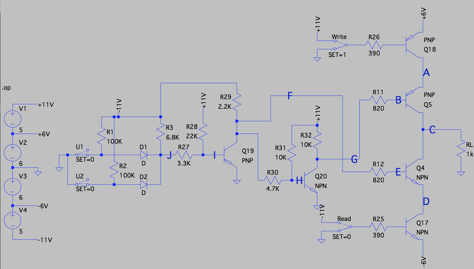
After some careful measurements, it became clear that the collectors of Q18 and Q5 had touched - they're VERY close on the board - and this had caused Q20 to fail shorted. I replaced Q20 with a 2N3904 and put heat-shrink tubing around Q5 on each of the 4 driver boards.